ABSTRACT
PbSe, Pb1-xEuxSe thin films and PbSe-Pb1-xEuxSe heterojunctions were successfully fabricated on ultrasonically cleaned glass substrates using molecular
beam deposition technic from a Knudsen cell made of high-purity graphite under a vacuum of 10-4 Pa and subsequently investigated. X-ray diffraction (XRD) patterns revealed
that all films exhibited dominant (200) peaks, indicating a highly textured structure. The surface morphology, concentration, and type of charge carriers depended on the
substrate temperature, the temperature of the additional compensating selenium source, and the deposition rate. It should be noted that, a transition from n-type to p-type
conductivity occurred at the additional compensating selenium source temperature (TSe) of 450 K. A smooth and uniform surface without clusters was achieved under the
following deposition conditions: θc=8÷9 Å/sec, Tsub=620 К.
Keywords: thin films, solid solutions, semiconductor, Pb1-xEuxSe.
DOI:10.70784/azip.1.2025353
Received: 12.09.2025
Internet publishing: 19.09.2025 AJP Fizika E 2025 03 en p.53-55
AUTHORS & AFFILIATIONS
1. Institute of Physics named after H.M. Abdullayev, Ministry of Science and Education of the Republic of Azerbaijan, 131 H. Javid Ave., Baku, AZ-1073, Azerbaijan
2. Azerbaijan Technical University, H. Javid ave., 25, AZ 1073, Baku, Azerbaijan
E-mail: afinnazarov@yahoo.com
Graphics and Images
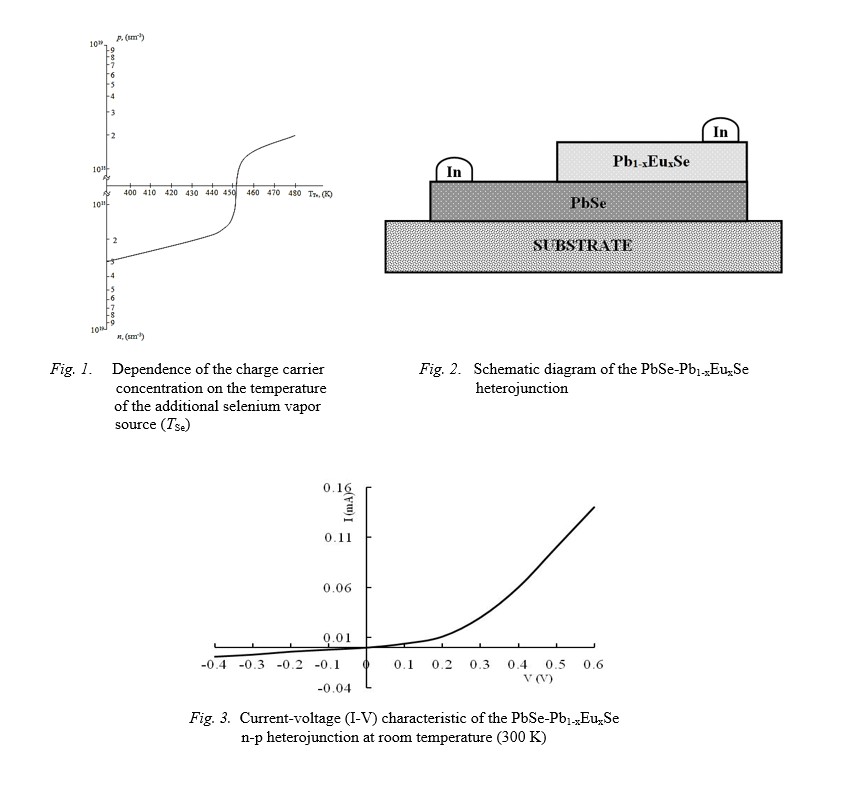
Fig.1-2-3
|
[1] E.A. Albanesi, E.L. Peltzery Blanca, A.G.Petukhov. Calculated optical spectra of IV–VI semiconductors PbS, PbSe and PbTe. Comput. Mater. Sci. Volume 32. Issue1, 2005, p. 85-95. https://doi.org/10.1016/j.commatsci.2004.07.001
[2] Asha Bhardwaj, E. Varadarajan, P. Srivastava, H.K. Sehgal. Structural, optical and electrical properties of chemically grown Pb1−xFexSe nanoparticle thin films. Solid State Commun. Volume 146. Issues1-2, 2008, p. 53-56. https://doi.org/10.1016/j.ssc.2008.01.021
[3] S.D. Delekar, M.K. Patil, B.V. Jadhav, K.R. Sanadi, P.P. Hanakare. Synthesis and characterization of Cd0.7Pb0.3Se thin films for photoelectrochemical solar cell. Solar Energy. Volume 84. Issue 3, 2010, p. 394-400. https://doi.org/10.1016/j.solener.2009.12.009
[4] V. Arivazhagan, M. ManonmaniParvathi, S.Rajesh. Impact of thickness on vacuum deposited PbSe thin films. Vacuum. Volume 86. Issue 8, 2012, p. 1092-1096. https://doi.org/10.1016/j.vacuum.2011.10.008
[5] I. Grozdanov, M. Najdoski, S.K. Dey. A simple solution growth technique for PbSe thin films. Materials Letters. Volume 38. Issue 1, 1999, p. 28-32. https://doi.org/10.1016/S0167-577X(98)00127-X
[6] D.K. Ivanou, E.A. Streltsov, A.K. Fedotov, A.V. Mazanik. Electrochemical depositionof nanocrystalline PbSe layers onto p-Si (100) wafers. Thin Solid Films. Volume 487. Issues1-2, 2005, p. 49-53. https://doi.org/10.1016/j.tsf.2005.01.033
[7] Vladimir Kasiyan, Zinovi Dashevsky, Casey Minna Schwarz, M. Shatkhin, Elena Flitsiyan, Leonid Chernyak, Dmitry Khokhlov. Infrared detectors based on semiconductor p-n junction of PbSe. J. Appl. Phys. Volume 112. Issue 8. 086101, 2012. https://doi.org/10.1063/1.4759011
|