ABSTRACT
The study investigates the impact of plasma-surface interaction on the structural, optical, and electrical properties of CuInSe2 (CIS) thin films. The films were
characterized using various methods, including atomic force microscopy, X-ray diffraction, absorbance, transmission, and electrical measurements. The results show that
plasma treatment significantly affects the electrical and optical properties of CIS films. The treatment increases transmission, decreases the absorption coefficient, and
decreases band gap energy values from 1.05 to 0.88 eV. The resistivity values of CIS films at room temperature decrease by three orders of magnitude after plasma treatment.
A planar cold microplasma device was used to visualize and record resistance inhomogeneity and photoconductivity distribution in a CuInSe2 copper-indium-diselenide
film. The plasma-induced damage (PID) in a CuInSe2 film is primarily attributed to the efficacy of sputtering and physicochemical interactions within the
discharge gap during the transition from Townsend to glow discharge. A nondestructive method was proposed for analyzing the kinetics of PID in the CuInSe2 film
using fractal processing within the planar cold microplasma device. Fractal dimension analysis was employed to quantitatively assess the alterations in dynamic
characteristics of the PID of CuInSe2 thin films. The film's quality was assessed through profile and spatially dispersed DLE intensity data, revealing surface
inhomogeneity and degradation over time.
Keywords: CuInSe2, X-ray diffraction, plasma-induced damage, thin film, discharge light emission, fractal dimension.
DOI:10.70784/azip.1.2025356
Received: 12.09.2025
Internet publishing: 24.09.2025 AJP Fizika E 2025 03 en p.56-66
AUTHORS & AFFILIATIONS
Institute of Physics, Ministry of Science and Education of the Republic of Azerbaijan, 131 H. Javid Ave., Baku, AZ-1073, Azerbaijan
E-mail:
Graphics and Images
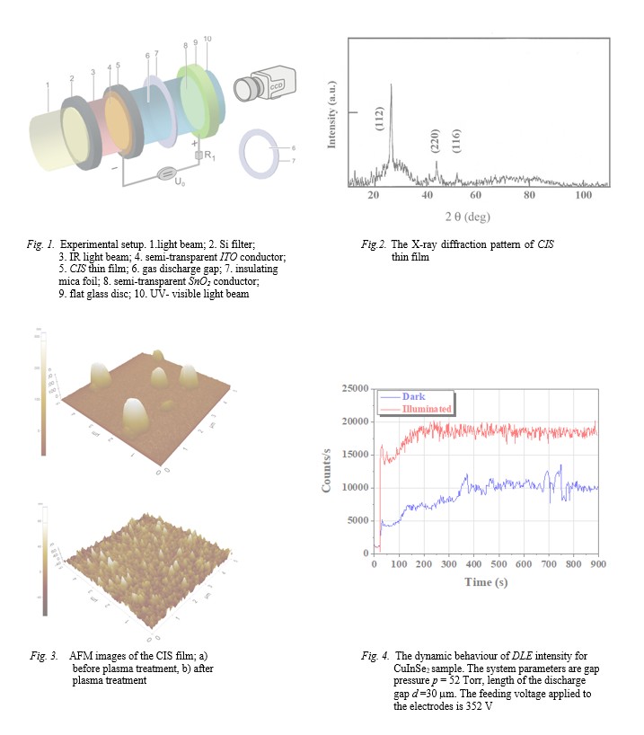
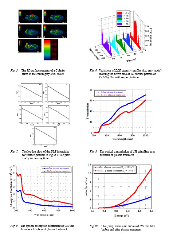
Fig.1-2-3-4 Fig.5-6-7-8-9-10
|
[1] Z.Z. Yan Zhang, Y. Liu, H. Gao, Y. Mao, Mater. Sci. Semiconduct. Process. 120, 105267, 2020.
[2] Z.Z. Yan Zhang, Y. Liu, H. Gao, Y. Mao. Organ. Electron. 67, 168–174, 2019.
[3] S.K.B. Joo Sung Kim, et al. Nano Energy 18, 30033–30038, 2018.
[4] T. Meyer, F. Engelhardt, J. Parisi and U. Rau. J. Appl. Phys. 91, 5093, 2002.
[5] I. H. Raja Azadar Hussain, Solid State Sci. 100, 106101, 2020.
[6] J. Müller, J. Nowoczin, H. Schmitt, Thin Solid Films 496(2):364-370 DOI:10.1016/j.tsf.2005.09.077 , 2006.
[7] H.Y. Kurt, E. Kurt and B.G. Salamov, Cryst. Res. Technol. 41, 698, 2006.
[8] E.L. Gurevich, S. Kittel, R. Hergenröder, Y.A. Astrov, L.M. Portsel, A.N. Lodygin, V.A. Tolmachev and A.V. Ankudinov. J. Phys. D: Appl. Phys. 43, 275302, 2010.
[9] K.S. Urmila, T.A. Namitha, B. Pradeep. Intern. J. Recent Research and Review (IJCRR) VIII(4), 6, 2015.
[10] Y. Wang and K. W. Xu. Thin Solid Films 468, 310-315, 2004.
[11] Z.W. Chen, X.P. Wang, S. Tan, S. Y. Zhang, and J. G. Hou. Physical Review B. 63, 165413 2001.
[12] K. Malek, Thin Solid Films 408, 73-78, 2002.
[13] H.Y. Kurt, E. Kurt, and B. G. Salamov, The Imaging Sci. J. 49, 205-212, 2001.
[14] B.G. Salamov, H. Y. Kurt, and E. Kurt, The Imaging Sci. J. 51, 187-197, 2003.
[15] H.Y. Kurt, E. Kurt, and B. G. Salamov, Cryst. Res. and Tech. 39 (9): 743-753, 2004.
[16] L. Gutay, D. Regesch, J.K. Larsen, Y. Aida, V. Depredurand, S. Siebentritt, Appl. Phys. Lett. 99, 151912, 2011.
[17] H.S. Min, S. Mandati, R. Chandran, A. Mallik, M. Arif, S. Bhuiyan, K.G. Deepa, Orient. J. Chem., 2019, 35, 01-13.
[18] M. Kemell, M. Rital, M. Leskel, Solid State and Mater. Sci., 2005, 30, 1–31, doi: 10.1080/10408430590918341.
[19] T. Feurer, R. Carron, G.T. Sevilla, F. Fu, S. Pisoni, Y.E. Romanyuk, S. Buecheler and A.N. Tiwari. Adv. Energy Mater. 2019, 9, 1901428, doi: 10.1002/aenm.201901428
[20] K. Tanaka, M. Kosugi, F. Ando, T. Ushiki, H. Usui and K. Sato, Jpn. J. Appl. Phys. 32, 113, 1993.
[21] S.M.F. Hasan, M.A. Subhan and K.M. Mannan, Opt. Mater. 14, 329, 2000.
[22] R. Jayakrishnan, T. Sebastian, T.T. John, C.S. Kartha and K.P. Vijayakumar, J. Appl. Phys. 102, 043109, 2007.
[23] R. Jayakrishnan, P.M. Ratheesh Kumar, C.S. Kartha and K.P. Vijayakumar, Meas. Sci. Technol. 17, 3301, 2006.
[24] J.-M. Cho, Journal of Nanoelectronics and Optoelectronics, 5, N 2, 218-221, 2010.
[25] B.G. Salamov and H. Yucel Kurt, J. Phys. D: Appl. Phys. 38 (5), 682-687, 2005.
[26] B.G. Salamov, A. Gunen., Imaging Sci. J. 49 (N 2), 101-111, 2001.
[27] L.V. Belyakov, A. Mageramov and L. G. Paritskii, Sov. Phys. Semicond. 12, 739, 1978.
[28] B.G. Salamov, K. Colakoglu and S. Altindal, Infrared Phys. & Technol. 36, 661, 1995.
[29] A.A. Akl and H.H. Afify, Mater. Res. Bull. 43, 1539, 2008.
[30] M.R. Balboul, A. Jasenek, O. Chernykh, U. Rau and H.W. Schock, Thin Solid Films 387, 74, 2001.
[31] S. Agilan, D. Mangalaraj, S.K. Narayandass and G. Mohan Rao, Physica B 365, 93, 2005.
[32] R.R. Philip, B. Pradeep, G.S. Okram and V. Ganesan, Semicond. Sci. Technol. 19, 798, 2004.
[33] L. Kronik, U. Rau, J.F. Guillemoles, D. Braunger, H.W. Schock and D. Cahen, Thin Solid Films 361, 353, 2000.
|